Our products
CVD Nano-Diamond Thick Film Bonding Tool
Product Features
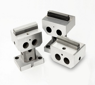
CVD Bonding Tool
Comparison the tip material between FONGSO TECHNOLOGIES and ANOTHER COMPANY
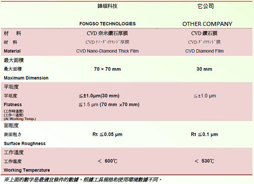
Comaprison of Tip Materials for Bonding Tool
Lots of makers, which are LCD manufacture, IC manufacture and MEMS manufacture, request the high competent bonding tool that has high efficient, high reliability and more affordable price. FONGSO TECH’s bonding tool adopts CVD Nano-Diamond Thick Film that our company has developed high quality and built up a mass production. FONGSO TECH is going to offer the expected bonding tool that is possible to realize the suitable bonding process, according to CVD Nano-Diamond Thick Film with high hardness, high heat conductivity and high precision process.
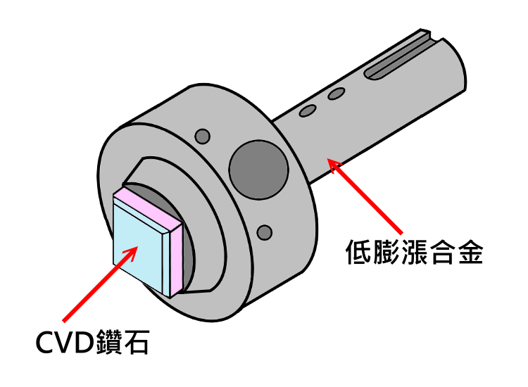
Structure
We should manufacture the shank of the bonding tool considering different heat expansion between CVD Nano-Diamond Thick Film and shank material. We adopt compound materials with low heat expansion ratio. We should adhere between CVD Nano-Diamond Thick Film and shank rigidly using special binder.
Design
TAB bonding tools are manufactured with high tolerance, under 1μm of the tip surface condition. We should take care of design the tool to restrict heat replacement of tip shape as minimum distortion by severe environment (Process temperature is about 400 ~ 600℃). We are possible to design optimum shank shape and tip form, according to process environment of customers. And then we prepare standard products.
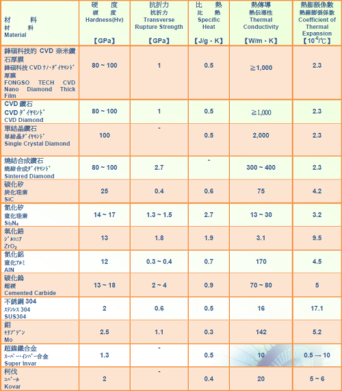
Heat properties CVD Nano-Diamond Thick Film
Diamond is the most high heat conductivity λ in the all materials. Heat conductivity of diamond is about 2.5 times against copper or silver at 300K (27℃). CVD Nano-Diamond Thick Film of FONGSO TECH possesses approximately 1000 W/mK at 600K. Such property is close to natural diamond.
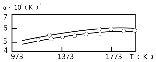
The heat expansion α of diamond is the most lowest in all materials. Such heat expansion coefficient α is
approximately ~ 1×10⁻⁶ K-1 at room temperature. The following figure indicate relationship between heat expansion coefficient
and temperature at high temperature
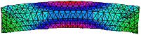
Flatness at high temperature
There is the different heat expansion between CVD Nano-diamond Thick Film and shank body. In case of process environment (high temperature etc.), tip flatness becomes distortion. Fongso Tech should restrict minimum distortion of tip flatness, according to tool design with buffer etc.
CVD Diamond Wafer of heat resistance
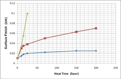
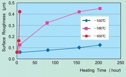
CVD Nano-Diamond Thick Film of FONGSO TECH possesses high heat resistance. However, using bonding tool in the atmosphere, surface layer of diamond or adhesion area are damaged by oxidizing. Please to take care of using. If you use the bonding tool under continuous process, you may take notice temperature up to 600℃.
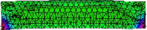
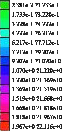
CVD Diamond Wafer of deviation of tip surface temperature
CVD Nano-Diamond Thick Film of FONGSO TECH becomes uniformity deviation of surface temperature, according to high heat conductivity. This leads to still more safety and reliability in bonding process.
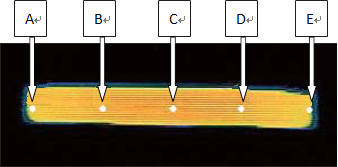
Controlled Temp:500℃ |
Fongso Tech |
A |
479℃ |
B |
483℃ |
C |
482℃ |
D |
483℃ |
E |
477℃ |
Max. |
483℃ |
Min. |
477℃ |
Temperature Distribution |
6℃ |