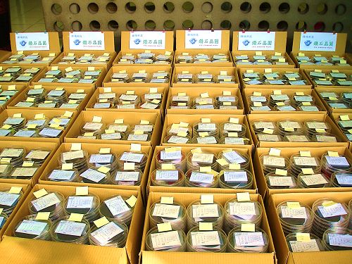
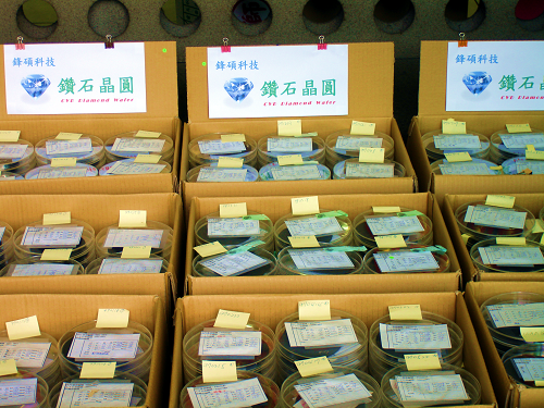
Our products
CVD diamond wafers
Applications
The developing trend of electronic consumer products must be getting compact size. Due to this trend, the circuit components must be designed for high density. Therefore, the heat issue will be a problem to electronic components. Electronic components will be malfunction or damage when the temperature is too high or with rapidly excessive heat. Using Alumina to have heat dissipation can’t increase the power of devices. Using copper to have heat dissipation will absorb too much waste heat to endothermic reaction.
Now, electronic and optoelectronic components power is increased to close the limitation of existing cooling package technology. In order to have power upgrade again in the future, we must solve the heat problem first, so how to choose good heat dissipation material is the key for the IC industry. Today, FongsoTech’s CVD diamond wafer is the ultimate heat spreading material can break through the current heat problems and bottle necks. Trust it will become the mainstream of future cooling materials. There are many applications can be applied to other high-tech industries.
| NO. | Function | Applications | Characteristics | Future Industry Applications |
| 1 | High-temperature semiconductors | Vehicles Aeroplane Control device for Turbine of industrial machine Control device for Home appliance |
Heat-resistance property |
Stable and reliable control at over 100℃ Miniaturization of home appliance |
| 2 | Substrate for high frequency / high power devices | Microwave wireless Lan(traffic control, communication in office environment, multiplex TV) High speed transistor High-speed data communication Non-contact entry door management |
High dielectric strength(withstanding voltage) High carrier drift mobility and saturation velocity |
High-spped, high-capacity data communication Optimization of traffic and entry Microwave amplifying device with GHz band |
| 3 | High-dielectric strength semiconductor | Power control | High breakdown voltage | Miniaturization of device |
| 4 | Electronic emission | Flat panel display | Negatively electron affinity | Low power consumption of display |
| 5 | Luminescence | Luminescence and laser from blue light to UV White light emitting Light source of printer |
Wide band gap | Large capacity optical recording Large size display Miniaturization of printer |
| 6 | Radiation detection | Digital X-ray image recorded Control of nuclear reactor |
Radiation resistance | Enhancement of roentgenology Maintenance of nuclear power generation |
| 7 | Optical detection | Fire detection UV monitor |
Wide band gap | Early detection of disaster Monitor of Global environment |
| 8 | Strain and pressure sensing | Super-sensitivity strain gauge and pressure sensor Strain gauge and pressure sensor with heat-resisting property |
Piezospecific resistance Heat-resisting property |
Super-sensitivity detector for industrial device |
| 9 | Temperature detection | Temperature sensor with super-sensitivity and radiation resistance | Wide band gap | Optimum combustion control of vehicle Maintenance of nuclear reactor |
| 10 | Magnetic field detection | Super-sensitivity magnetic field sensor Rotation detection of vehicle, aeroplane, turbine |
Magneto-resistance effect | Optimum control of rotator |
| 11 | Window of x-ray | mask of photolithograph | High luminous transmittance | Manufacture of sub-micron LSI |
| 12 | Window of infrared ray | Window of infrared ray | High luminous transmittance | Monitor of global environment |
| 13 | Thermal diffusion | Heat sink | High thermal conductivity | Improvement of reliability for microwave module |
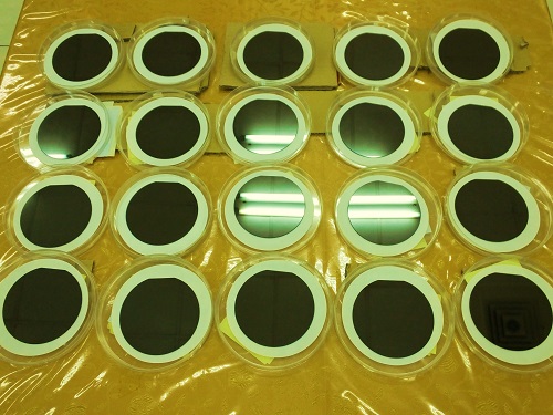
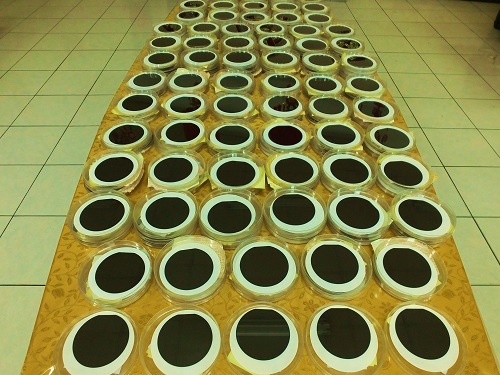
CVD diamond wafer
Fongso Technologies : 4-inch CVD Diamond Film on Si Substrate as non-polish

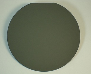
Fongso Technologies : 4-inch CVD Diamond Film on si substrate as mirror polish (Surface finish Ra 1.052nm Rq 1.321nm)
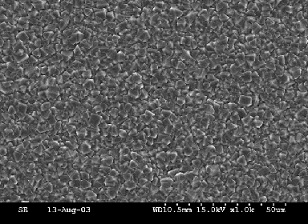
Fongso Technologies : SEM image of 4-inch CVD Diamond Wafer Surface as non-polish (Magnification : 1,000 times)
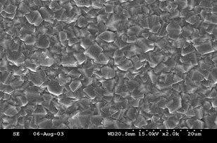

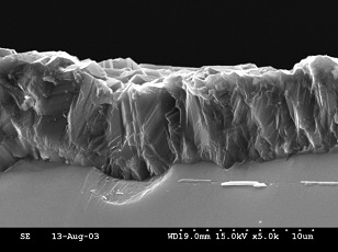
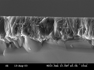
Fongso Technologies : SEM image of 4-inch CVD Diamond Wafer cross-section as non-polish