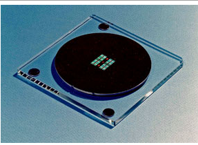
CVD diamond wafer applications
摻硼鑽石電極
Boron-doped diamond electrodes
絕緣閘雙極性電晶體(IGBT)
Insulated Gate Bipolar Transistor (IGBT)
CVD鑽石工具和UPC工具
CVD Diamond tool & UPC tool
AMF & STM的描畫針
Stylus for AMF & STM
光學機器的X射線視窗
Optical device X-ray window
高敏感的半導體傳感器
High sensitive semiconductor sensor
Lithographic Photomask
為半導體的平版印刷遮蔽物
Lithographic photomasks are typically transparent fused silica blanks covered with a pattern defined with a chrome metal absorbing film.
Lithographic photomasks are used at wavelengths of 365 nm,248 nm and 193 nm.
Lithographic photomasks have also been developed for other forms of radiation such as 157 nm, 13.5 nm (Extreme Ultra Violet:EUV), X-ray and electrons and ions.
Diamond membrane is expected for new materials of the photomasks,because diamond has good mechanical strength.That means diamond has high durability against SR (Synchrotron Radiation)exposure with long lifetime,Young's modulus required for accurate pattern positioning.

Photo lithography mask for x-ray
Application
Semiconductor device, Flat panel display and Print circuit board etc.
Price (World market)
1 mask set for 45 nm : 200 million JPY(2)
Reference
(1) Wikipedia : Photomask
(2) weblio Wikipedia
